Processor development
A reduced FPGA implementation has reproducible simulation, selected formal checks and tool-generated build evidence. The full custom processor remains under development.
 AMERICAN ARCHON™MOTHERBOARD · PROCESSOR · SOFTWAREInvestor login
◆ AMERICAN ARCHON™ PROCESSOR
JR Morales’s vision is a revolutionary proprietary motherboard, processor and software platform intended to reshape computing and AI. Its central development goals are lower energy per completed workload and substantially higher processing throughput, with processor design and proprietary HexOS software developed together. These goals are not yet measured hardware results. A reduced FPGA/software checkpoint has passed reproducible build and scoped verification checks; physical hardware validation remains outstanding.

01 / TECHNOLOGY
American ARCHON™ is being developed as an integrated processor and proprietary software platform. Its intended differentiation comes from the coordinated relationship among processor design, HexOS, memory handling and specialized execution methods. Detailed mathematics, algorithms, source code, RTL and enabling implementation details remain confidential.
The November 16, 2026 audit establishes an incomplete engineering checkpoint. HexOS currently comprises host/runtime and simulation capabilities rather than a completed bootable operating system. QuantumMode currently provides classical software modeling, not physical quantum-computer validation.
A reduced FPGA implementation has reproducible simulation, selected formal checks and tool-generated build evidence. The full custom processor remains under development.
The proprietary host/runtime and simulation environment is intended to coordinate platform capabilities. A complete bootable operating system has not been demonstrated.
Current evidence is classical software modeling and testing. It does not establish physical quantum processing or measured quantum advantage.
02 / PROCESSOR & CONNECTION ARCHITECTURE
Updated illustrations communicate the processor and proprietary software vision without exposing enabling implementation details. Concept artwork is separate from verification evidence. These are not manufacturing drawings or physical prototype photographs.
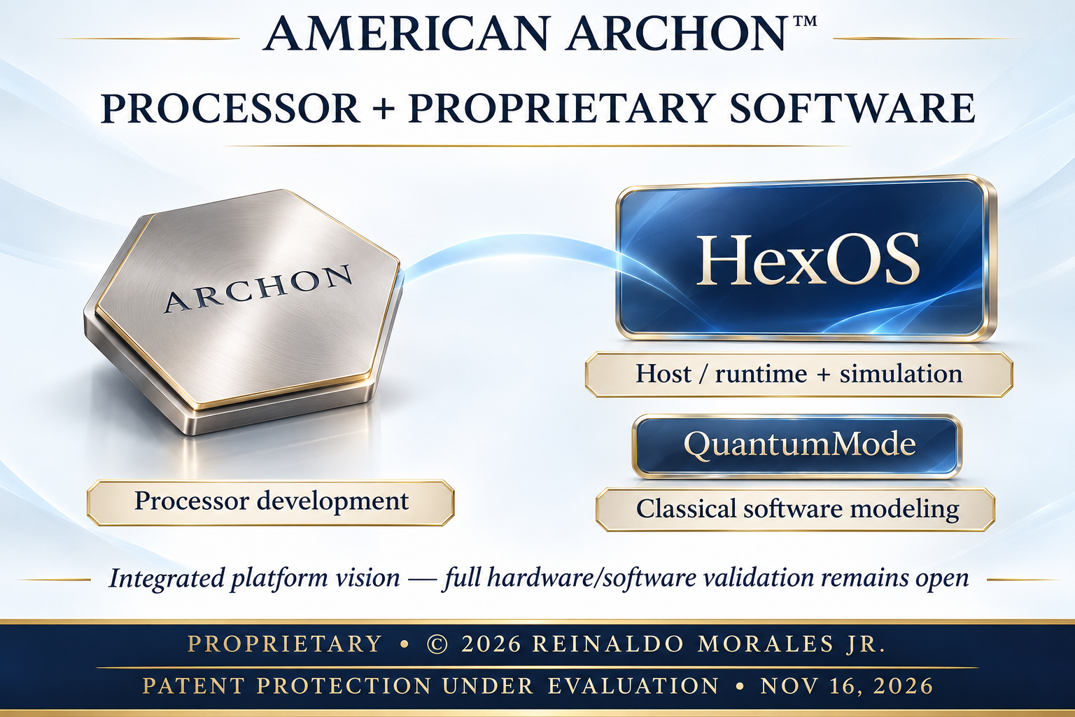

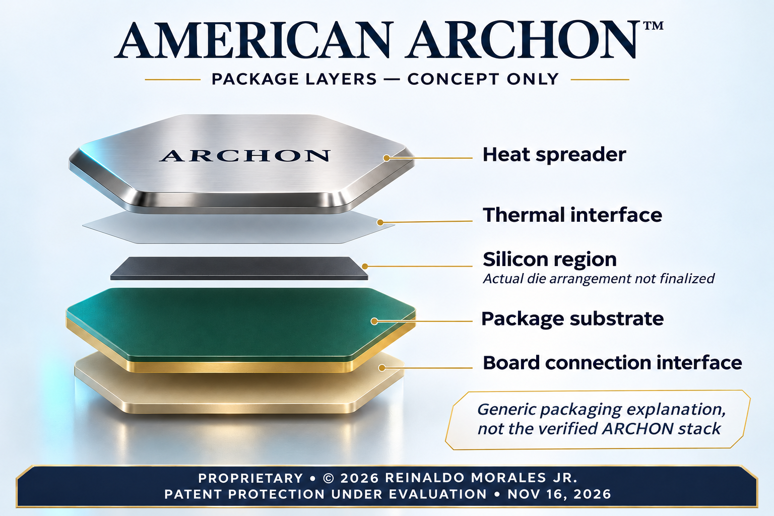

The updated illustrations communicate the development vision. Historical originals are preserved separately. They do not disclose the authoritative mathematics or implementation and must not be used to infer verified interfaces, timing, pin assignments, physical placement or manufacturability. The restricted engineering baseline, verification evidence and remaining defects are maintained separately.
03 / PROTOTYPE MOTHERBOARD
The ARCHON Prototype Motherboard™ is a regular rectangular motherboard platform. It is not a hexagonal motherboard.
The artwork depicts a six-sided ARCHON Q processor package on a conventional rectangular motherboard. Socket engineering, electrical interfaces, placement, routing and manufacturing checks remain unfinished. No assembled or tested motherboard is asserted.
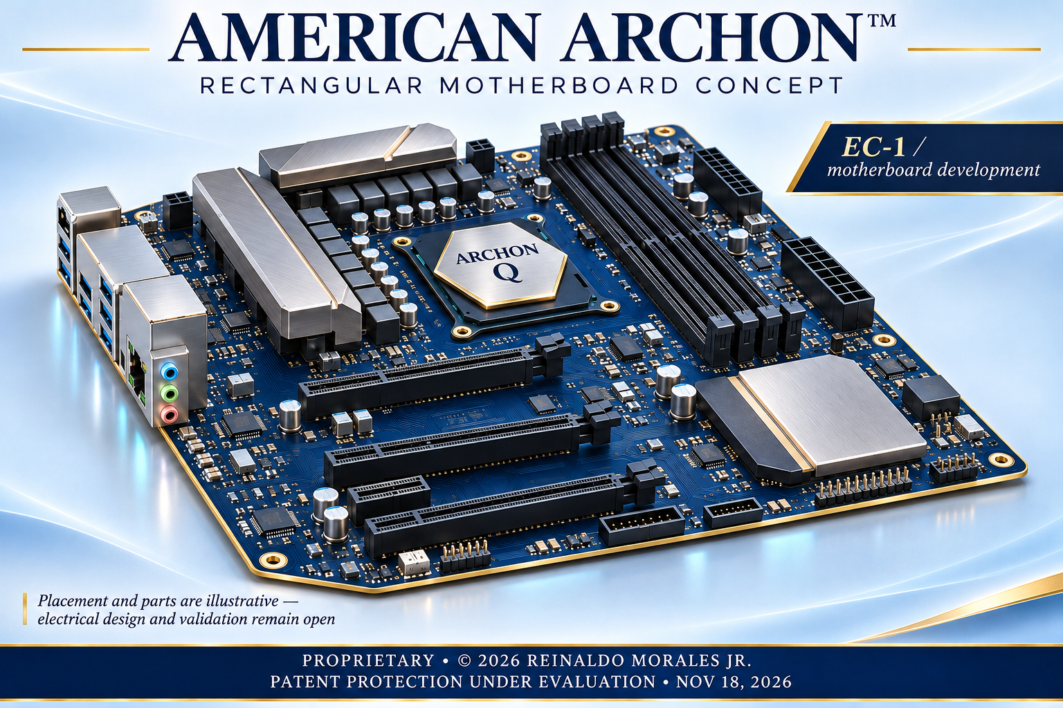
The rectangular motherboard concept considers memory, power delivery, storage, expansion, networking, cooling, firmware and diagnostics. These are proposed functions, not installed or tested capabilities. EC-1 and motherboard completion requires native schematics, PCB layout, BOM, integrity analysis, electrical/design-rule checks, assembly outputs and qualified review. The following subsystem descriptions are planning items.
Proposed central processor zone and retention concept within a conventional rectangular motherboard; implementation remains open.
Cold plate, vapor or liquid cooling, fan and pump control, sensor rings and shutdown.
ECC-capable channels, regulated power, module identification and thermal monitoring.
Reserved future near-processor high-bandwidth memory zone; HBM is not claimed as installed.
ATX/EPS input, staged voltage conversion, current sensing, protection and sequencing.
x16, x8 and x4 pathways for accelerators, storage, networking and lab cards.
Reconfigurable logic, configuration flash, JTAG and mezzanine validation interfaces.
Dual BIOS, recovery controls, board management, watchdogs and sensors.
JTAG, UART, POST display, safe boot, probe pads and dummy-load connectivity.
TPM 2.0, secure boot, debug lockout, precision clocks and audit path.
NVMe, optional U.2/EDSFF and SATA; USB4, service USB-C and Ethernet.
Controlled-impedance layers, power planes, mounting, reinforcement and cooling support.
03 / PERFORMANCE & COMPARISON
The exact revision 0.2.0 checkpoint package passed a clean-extraction run: 73 Python tests, RTL benches in Icarus and Verilator, selected bounded/combinational formal checks, and FPGA synthesis, placement, routing and bitstream generation with matching output hashes. These results cover a reduced FPGA/software scope.
ENERGY EFFICIENCY + PROCESSING SPEED
Reducing energy per completed task is a central ARCHON design goal, alongside faster processing. The intended benefit is more AI and computing work within practical power and cooling limits. The size of any saving or speed increase has not been established by physical ARCHON measurements.
A fair CPU/GPU comparison must run the same workload at equal accuracy and quality, record elapsed time, and measure energy across the same system boundary. Chip power alone cannot establish total system savings. No verified percentage reduction, speed multiplier or exponential speedup is claimed.
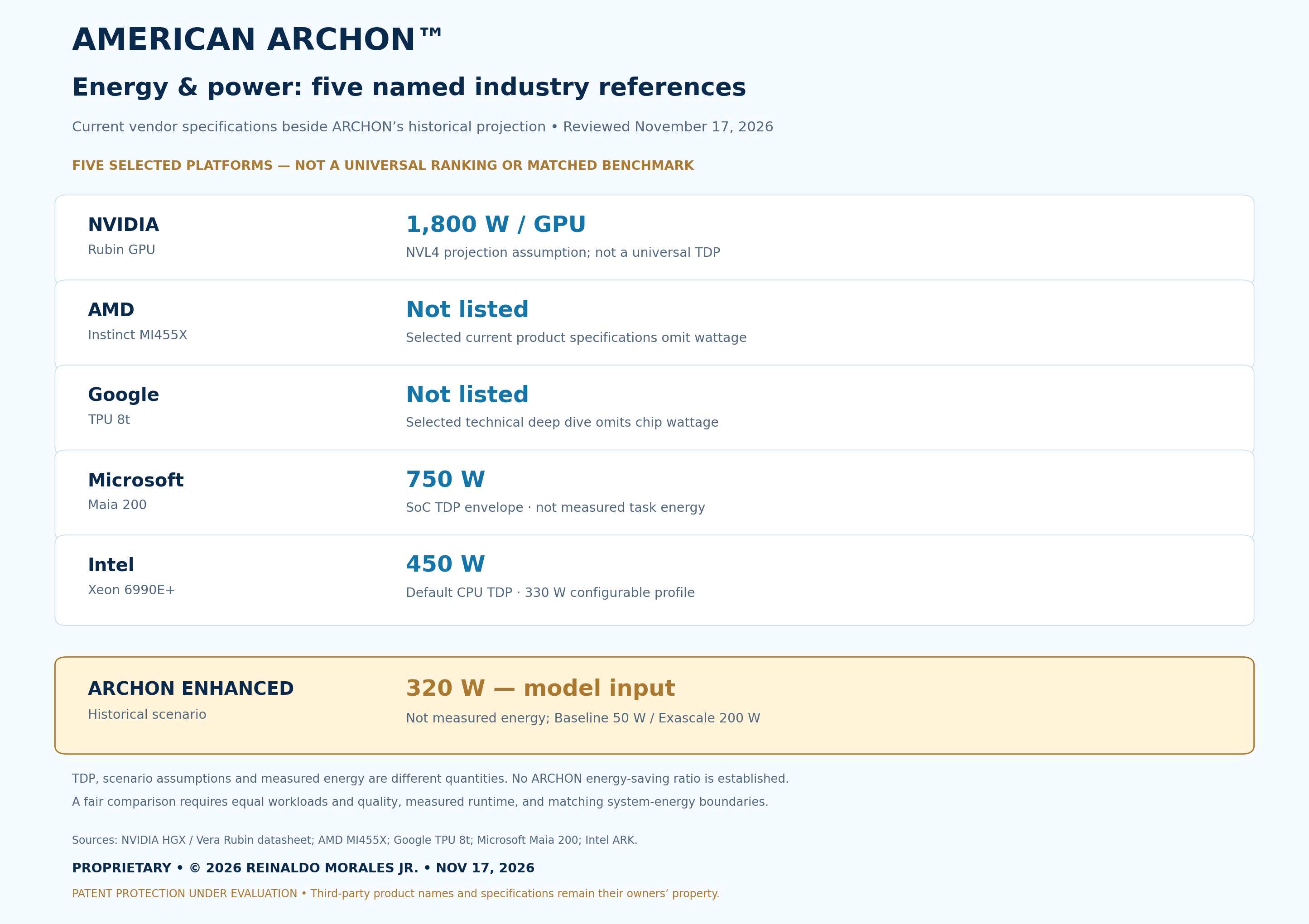
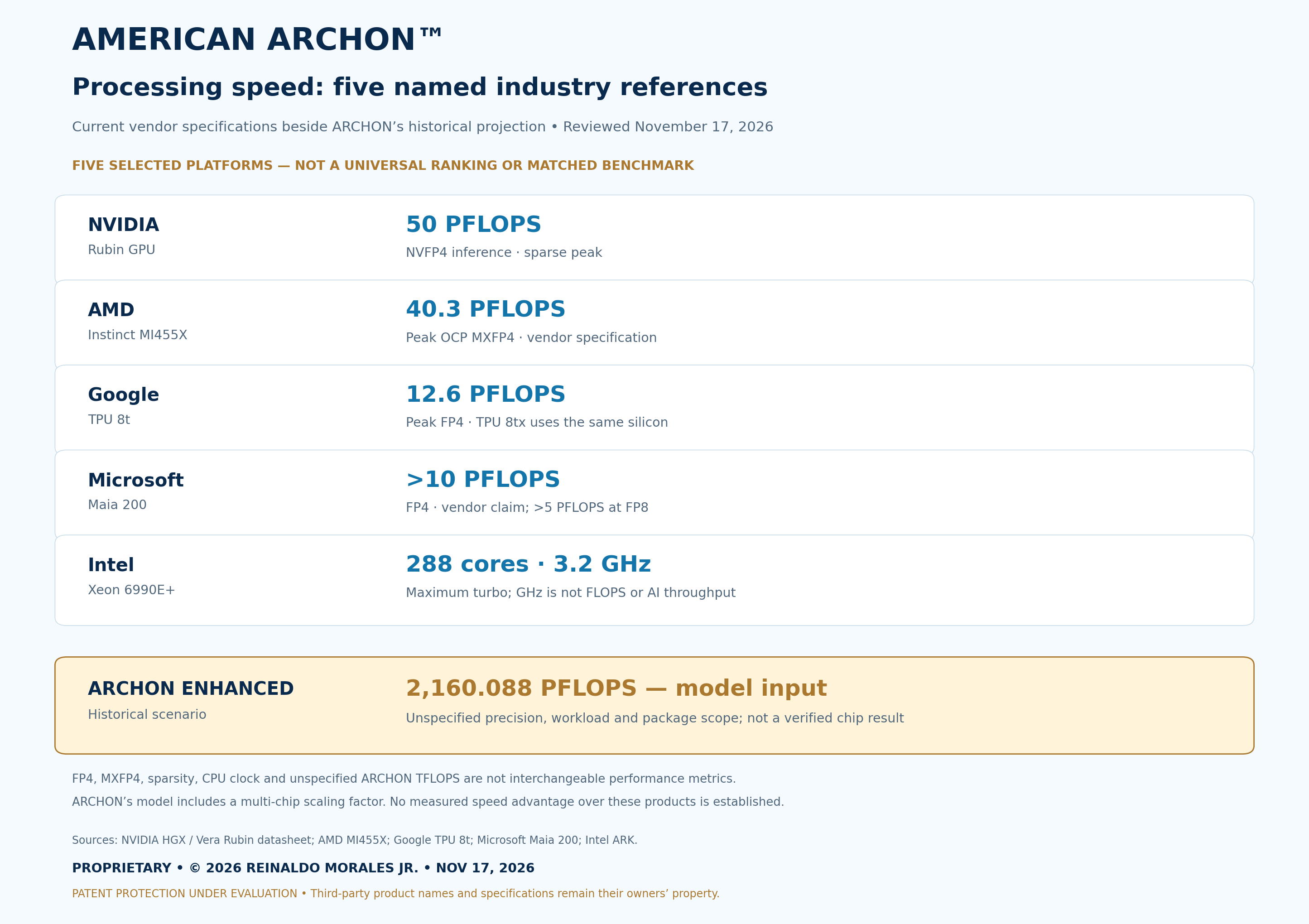
Selected prominent platforms, reviewed November 17, 2026; not an exhaustive or universal top-five ranking. GPU/TPU peaks, CPU clock rates and the ARCHON scenario are not equivalent tests. Google’s November 9 additions are TPU 8tx and TPU 8i Max system configurations; 8tx uses TPU 8t silicon.
| Platform | Published performance | Power category | Primary evidence |
|---|---|---|---|
| NVIDIA Rubin GPU | 50 PFLOPSNVFP4 inference · sparse peak | 1,800 W / GPUNVL4 projection assumption; not a universal TDP | Manufacturer source · Power assumption |
| AMD Instinct MI455X | 40.3 PFLOPSPeak OCP MXFP4 · vendor specification | Not listedSelected current product specifications omit wattage | Manufacturer source |
| Google TPU 8t | 12.6 PFLOPSPeak FP4 · TPU 8tx uses the same silicon | Not listedSelected technical deep dive omits chip wattage | Manufacturer source · New configurations |
| Microsoft Maia 200 | >10 PFLOPSFP4 · vendor claim; >5 PFLOPS at FP8 | 750 WSoC TDP envelope · not measured task energy | Manufacturer source |
| Intel Xeon 6990E+ | 288 cores · 3.2 GHzMaximum turbo; GHz is not FLOPS or AI throughput | 450 WDefault CPU TDP · 330 W configurable profile | Manufacturer source |
| ARCHON Enhanced | 2,160.088 PFLOPSHistorical model input; unspecified precision; multi-chip factor in scaling | 320 WModel input; not measured silicon or task energy | Recovered enhanced master summary and scaling pathway |
Comparison gate: An ARCHON advantage remains unverified until the same workloads, arithmetic precision, accuracy, sparsity, system boundaries and measured energy are matched. No speedup or energy-saving percentage against these products is established.
Tool-build setting, not measured board performance or a custom-silicon clock rating.
Software, RTL and selected formal properties passed under documented assumptions. Full coverage remains open.
No physical FPGA or fabricated-silicon performance, power or competitor advantage is certified.
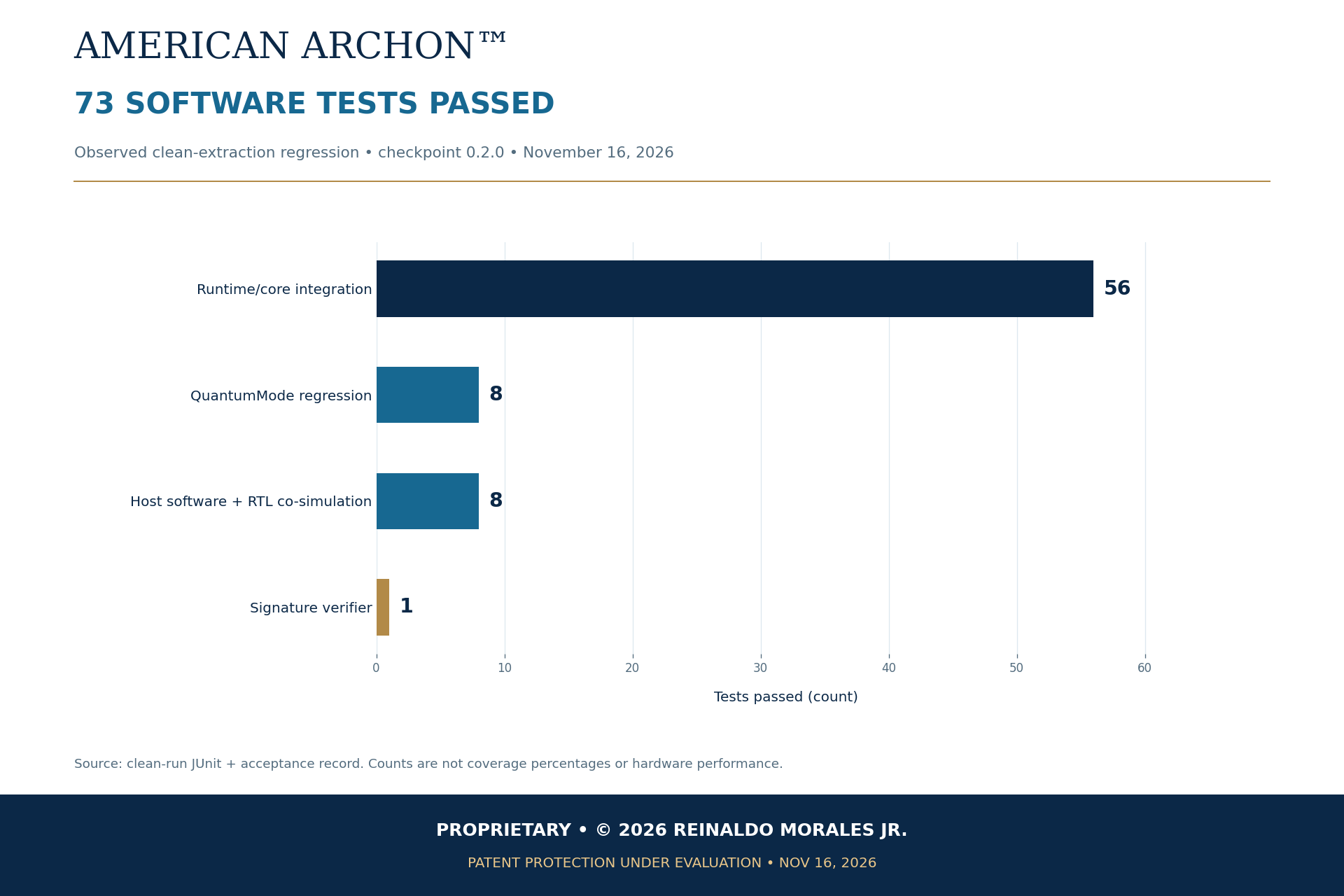
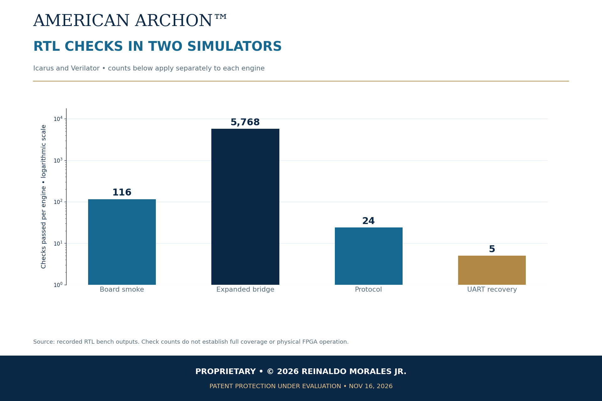
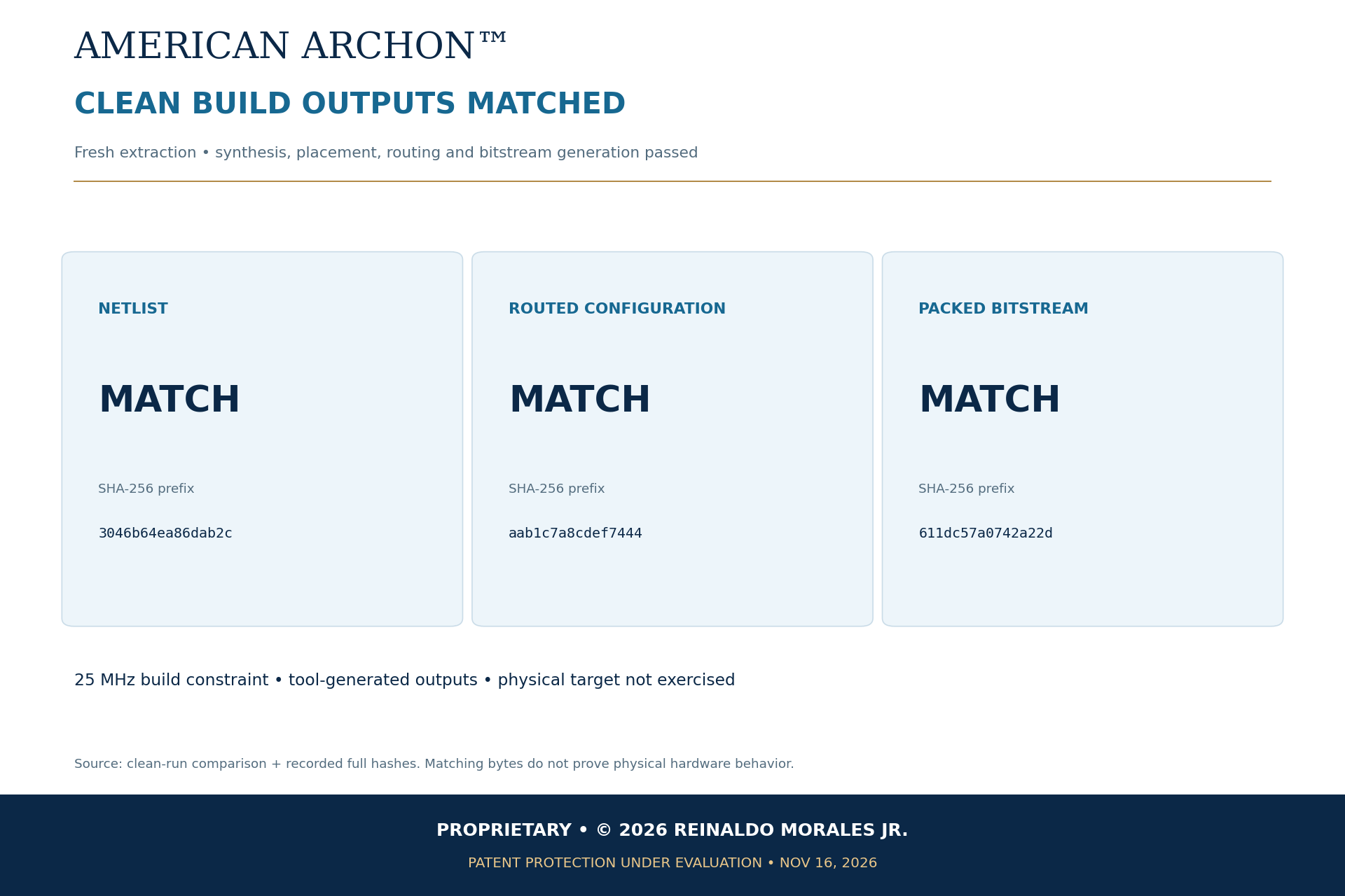
High-level development concepts only; this table establishes no performance advantage.
American ARCHON™ is intended to combine processor design and proprietary software as one coordinated platform. Comparative performance remains a research and validation objective; no independently measured advantage is established.
Historical performance figures and artwork labels are concepts, models or targets, not certified hardware measurements. Current software tests, RTL simulation, scoped proofs and FPGA tool outputs must each be assessed within their own verification category.
04 / HEXOS & QUANTUMMODE
HexOS is the dedicated environment intended to control, coordinate or expose the processor’s capabilities. The recovered implementation currently includes host/runtime and simulation functionality. QuantumMode provides classical software modeling. Their relationship to the processor is part of an integrated development program; neither name establishes completion of an operating system or quantum hardware.
QuantumMode software results are not physical quantum-computer validation. No qubit-based processor, quantum advantage, completed operating system or physical motherboard operation is claimed. Proprietary equations, algorithms, code and enabling interfaces are withheld from public disclosure.

05 / MANUFACTURING & VALIDATION
Current status: INCOMPLETE ENGINEERING CHECKPOINT — revision 0.2.0, reviewed November 16, 2026. A reduced ULX3S / ECP5-85F build is reproducible. Generalized specification authority, physical FPGA tests, complete platform implementation, production security and qualified signoff remain open. The following lists are future acceptance stages, not completed milestones.
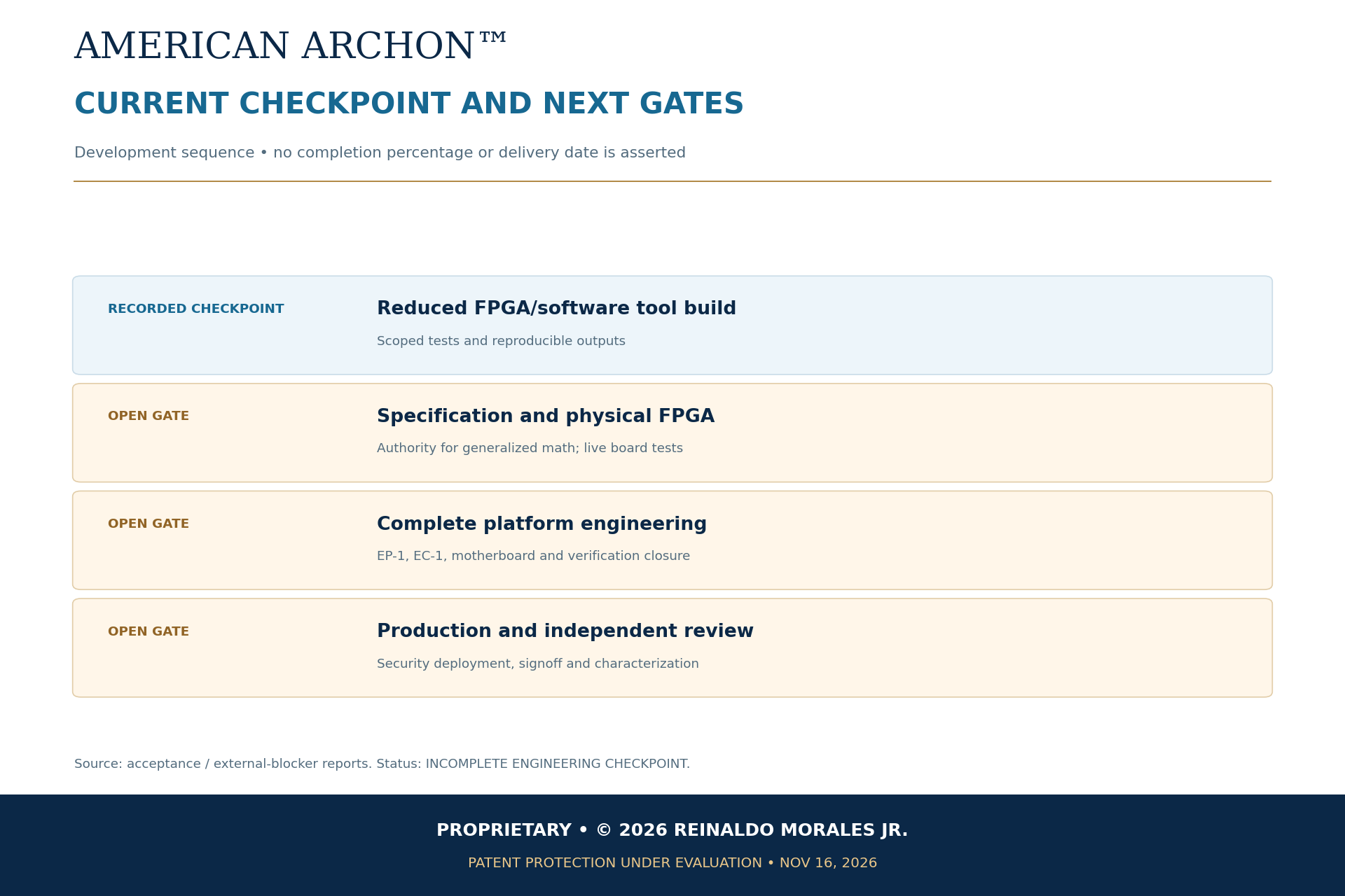
Next gate: Complete native electrical design, engineering review and manufacturer-specific acceptance checks; no supplier engagement is asserted.
Next gate: EP-1 implementation and verification closure, process/IP selection, physical design, package planning and foundry-qualified signoff; no tape-out readiness is asserted.
INVESTOR & STRATEGIC PARTNER BRIEF
American ARCHON is seeking conversations with seed investors and engineering partners to move the integrated motherboard, processor and proprietary software program toward a working, measured hardware platform.
The immediate purpose is practical: establish a controlled engineering baseline, complete board design, continue verification and prepare independently reviewable hardware evidence.
Resolve specification and interface gaps, select the reproducible source baseline, expand regression coverage and commission qualified engineering review.
Acceptance evidenceReviewed requirements, source hashes, build instructions, test results and a tracked defect register.
Complete native schematics, PCB layout, component selection, BOM, power and clock planning, manufacturing checks and supplier quotations.
Acceptance evidenceReviewed ECAD files, ERC/DRC results, priced BOM and approved fabrication and assembly outputs.
Acquire the target FPGA board and laboratory resources, fabricate the reviewed prototype board when ready, and test reset, power, firmware, memory and I/O.
Acceptance evidenceBoard identity, programming records, bring-up logs, instrument captures and reproducible pass/fail results.
Run matched workloads at equal accuracy. Measure elapsed time and system energy, document thermal behavior and seek independent technical review.
Acceptance evidenceVersioned benchmark methods, raw measurements, limitations and an independent review report.
Processor/RTL and verification engineers; PCB and power specialists; firmware and host/software integration; EDA tools; FPGA hardware; laboratory equipment; fabrication and assembly partners; independent reviewers; and intellectual-property counsel.
The existing $10M foundational stage below belongs to the broader preliminary capital roadmap. A smaller seed tranche has no approved amount or terms on this site. Its scope, quotations, milestones, contingency and reporting schedule must be agreed before a commitment.
A non-enabling overview, checkpoint scope, planned use of funds, milestone acceptance criteria, remaining risks and team/resource needs. Restricted implementation materials require separate authorization and controlled review.
Physical-board validation, complete platform integration, manufacturability, cost and schedule remain unresolved. Claimed energy or speed advantages require measurement. Custom silicon is a later stage requiring its own tools, partners and signoff.
Exploratory investor and partnership inquiries only. No payment, share purchase or investment commitment is accepted here. Offering terms and definitive documents require separate approval; no financial return or development outcome is guaranteed.
06 / PRIVATE CAPITAL ROADMAP
The planned pathway funds the complete development program from essential-team formation through FPGA validation, first silicon, preproduction and controlled initial production. Amounts are preliminary and subject to engineering review, quotations, financing terms and board approval.
Foundational engineering, the seven-person core team, architecture, RTL, motherboard planning, IP protection and operating runway.
FPGA implementation, rectangular prototype motherboard, firmware, diagnostics and independent functional testing.
ASIC physical design, tape-out, fabrication, packaging, first-silicon bring-up and laboratory testing.
Design corrections, expanded validation, production motherboard and controlled preproduction preparation.
Initial production, customer-evaluation systems, manufacturing controls and future public-market readiness.
The sign-in portal describes the preliminary review pathway. Private documents are pending assignment; qualification and funding providers are not active. This public page is informational and is not an offer to sell securities.
07 / IP PROTECTION
Public materials communicate the investment thesis without exposing processor internals, schematics, source code, algorithmic structures, simulation code or manufacturing secrets.

08 / INVESTOR INQUIRY
Qualified investors, strategic partners, semiconductor manufacturers, government stakeholders and engineering-review partners are invited to request a controlled introduction.
jrmorales.net@gmail.com09 / LEGAL NOTICE
The information on this website is provided for preliminary informational and discussion purposes only. It does not constitute an offer to sell securities, a solicitation to buy securities, investment advice, legal advice, engineering certification, or a guarantee of technical performance.
All technical descriptions, performance projections, quantum-calculation claims, development plans, funding estimates and manufacturing pathways are preliminary and subject to engineering review, legal review, third-party validation, prototype testing and manufacturing feasibility analysis.
Historical performance figures and artwork labels are concepts, models or targets, not certified hardware measurements. Current software tests, RTL simulation, scoped proofs and FPGA tool outputs must each be assessed within their own verification category.
Detailed processor design, software, algorithmic structure, simulation materials, documentation and engineering files may require NDA protection and controlled confidential review.